Samsung chip plant spurs $30bn more investment in Korea
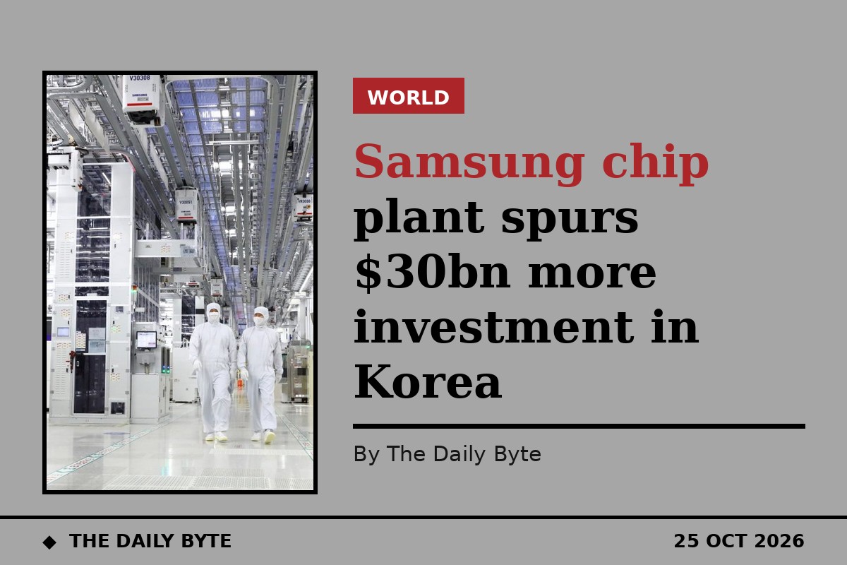
South Korea's President Lee Jae Myung has said Samsung Electronics' new chip packaging plant in Asan will trigger about 40 trillion won (about $30 billion) of further investment in advanced equipment, in a major boost for the country's semiconductor industry.
Lee made the announcement on Thursday at a groundbreaking ceremony at Samsung's Onyang Campus in Asan, where the company is building a 6 trillion won ($4.48 billion) plant to package high-bandwidth memory (HBM) chips used in artificial intelligence servers.
The president said South Korea would become a core hub for advanced HBM packaging, as demand for the high-performance memory that powers AI data centres continues to grow sharply.
Production to start in June 2028
Samsung said the new HBM production line is scheduled to begin operations in June 2028, a year earlier than initially planned, as it races to meet rapidly growing demand for server memory.
The plant will have three floors of clean-room space covering about 31,000 square metres, according to a company presentation at the ceremony.
The investment is part of plans announced by Samsung affiliates in July, which also include a high-tech display production line and a facility in Sejong making high-performance substrates for AI servers.
Why HBM packaging matters
High-bandwidth memory is stacked and packaged alongside AI processors, and advanced packaging has become one of the most competitive parts of the chip supply chain as AI companies demand faster and more efficient memory.
South Korea is already home to the world's two largest memory chip makers, Samsung Electronics and SK hynix, and the government has been pushing to strengthen the country's position in advanced packaging and other parts of the AI hardware supply chain.
The Asan project sits in South Chungcheong province, where the government and Samsung are developing a wider semiconductor and display cluster.
What happens next
Construction is now under way at the Onyang Campus, with the new line due to start production in mid-2028. The follow-on equipment investment of about 40 trillion won is expected to flow in as the facility is fitted out and production ramps up.